Why Chiplets Are Everywhere All of a Sudden
For decades, computing progress depended on shrinking transistors on a single piece of silicon. That simple playbook is running out of room. Costs climb, yields fall, and the physical limits of lithography stare back. Yet demand for performance keeps climbing thanks to AI, gaming, simulations, and cloud services. The solution showing up across product lines—from data center processors to high-end phones—is not just “a smaller chip.” It’s a new way to build chips altogether.
This approach, often called “chiplets” or “advanced packaging,” splits a large chip into smaller, specialized pieces and wires them together at extremely short distances inside the same package. Instead of one enormous die doing everything, you get a cluster of smaller dies working as a team. It sounds simple, but the consequences are big: better performance per watt, lower costs from higher yields, faster iteration, and the freedom to mix manufacturing processes.
That’s why you’re seeing terms like 3D packaging, UCIe, HBM, and Foveros in product announcements. They are not buzzwords for the sake of it. They describe how the industry is rebuilding computing from the bottom up to keep progress moving.
What “Chiplet” Actually Means
From Monoliths to Modules
A traditional system-on-chip (SoC) tries to pack everything—CPU cores, GPU units, memory controllers, I/O—onto one die. That works until the die gets too big. Large dies have lower yields because there’s a higher chance that any given defect ruins the whole chip. They also hit the reticle limit, the maximum area that lithography tools can print at once.
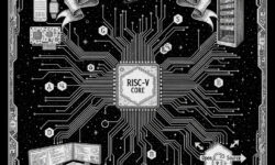
Chiplets break the SoC into smaller dies that each handle a function: compute, I/O, cache, memory, accelerators. These dies are placed side-by-side or stacked and interconnected inside one package. The package then looks like a single chip to the outside world, even though it contains several.
2.5D vs. 3D, in Plain Language
- 2.5D packaging: Multiple dies sit side-by-side on an interposer (a thin slice of silicon or another material) that carries thousands of tiny wires between them. Think of it as a dense “circuit board” at microscopic scale.
- 3D packaging: Dies are stacked vertically and connected through through-silicon vias (TSVs), which are tiny vertical wires passing through silicon. This brings components closer than any circuit board could.
Both options slash distances and boost bandwidth compared to separate chips on a motherboard. These approaches are sometimes combined: a 2.5D interposer can host side-by-side dies, and each die might be a 3D stack internally.
The Economics Behind the Shift
Yield, Cost, and the Reticle Wall
Semiconductor manufacturing statistics are unforgiving. A small defect can scrap a large die, but it might only scrap one out of several smaller dies. If you build with chiplets, you test each die, keep the good ones (known-good-die, or KGD), and assemble them into finished parts. The result is a higher effective yield and lower cost per functioning square millimeter of silicon.
There’s also the reticle limit: you can’t pattern a die larger than the field a lithography tool can expose. Very large monolithic designs simply don’t fit. Chiplets jump over that barrier by stitching multiple smaller dies together in-package.
Mixing Process Nodes to Save Money
Not every function needs the most expensive, cutting-edge manufacturing. You may want the latest node for CPU or AI cores, but not for USB controllers or PCIe lanes. Chiplets let you put the most demanding logic on an advanced node while keeping I/O or analog on older, cheaper nodes. You can even reuse a proven I/O chiplet across several generations of compute dies.
Speeding Up Product Cycles
If one chiplet improves—say, a new compute tile—you can upgrade the product without redesigning everything. That modularity reduces time-to-market and lets companies create more product variants: fewer SKU-specific monoliths, more building-block combinations.
Inside the Package: The Wiring That Makes It Work
UCIe: A Common Language for Chiplets
High-bandwidth chiplet systems need fast, efficient, standard ways to talk between dies. That’s where UCIe (Universal Chiplet Interconnect Express) comes in. UCIe defines how dies connect and exchange data, much like PCIe standardized communication between host and add-in devices. With UCIe, a compute tile from one vendor could, in principle, talk to a memory or accelerator tile from another—paving the way for a broader chiplet ecosystem.
Before UCIe, companies used bespoke links such as AMD’s Infinity Fabric or proprietary short-reach PHYs. Those work but limit cross-vendor compatibility. Standards don’t guarantee plug-and-play overnight, but they open the door.
Other Short-Reach Links You’ll Hear About
- BoW (Bunch of Wires): A pragmatic, open specification favored for simplicity in certain chiplet scenarios.
- OpenHBI: An interface focused on memory-like chiplets and high-density connections.
- Company-specific links: Highly tuned, proprietary interconnects that squeeze out maximum performance for a particular architecture.
Under the hood, these links are optimized for ultra-short distances and high energy efficiency, delivering terabytes per second of bandwidth per package with far less energy than traditional off-package connections.
Memory Is the New Battleground
HBM: Stacked Memory, Sky-High Bandwidth
High-Bandwidth Memory (HBM) is the go-to companion for modern AI accelerators and enterprise CPUs. Instead of spreading memory out as separate chips on a motherboard, HBM stacks multiple DRAM layers vertically and connects them to the processor using an interposer with thousands of fine-pitch wires. The result is massive bandwidth at lower power per bit moved.
Current systems use HBM2E, HBM3, and HBM3E, with HBM4 on the horizon. Each generation increases bandwidth per stack and often capacity, but it also demands more advanced packaging and careful thermal design. HBM doesn’t replace all types of memory—systems still use DDR or LPDDR for capacity—but it transforms performance in bandwidth-hungry workloads like training neural networks or real-time analytics.
Why Bandwidth per Watt Beats Raw MHz
Moving data is expensive. As clock speeds plateau, systems gain more by making data movement shorter and wider. HBM delivers more bandwidth per watt than traditional DIMMs by living inside the package and shortening every signal path. Chiplets plus HBM concentrate compute and memory bandwidth in a compact area. That compactness is a double-edged sword—it squeezes out performance but intensifies heat and power integrity challenges.
Heat, Power, and the Practical Limits
Thermal Density: Performance’s Shadow
Putting many high-performance dies and stacked memory in one package creates hotspots. Designers need better thermal interface materials, heat spreaders, and power delivery schemes to keep temperatures in check. Thermal simulations tend to drive floorplans: you can’t place the hottest chiplets shoulder-to-shoulder without a plan for heat extraction.
Power Delivery in 2.5D/3D
Power distribution must feed multiple hungry dies while keeping voltage ripple low. An interposer adds routing flexibility—and resistance. Engineers carve thick power rails, use additional bumps, and sometimes dedicate layers to power and ground to ensure steady, low-noise delivery. The challenge grows with each added HBM stack and compute tile.
Designing a Chiplet System Is Not Just “Cut and Paste”
Partitioning: What Goes Where
The art of chiplet design starts with partitioning. Teams identify blocks that benefit from advanced nodes versus those that don’t. They map out bandwidth needs between blocks and reserve the fattest, shortest connections for the noisiest traffic. They also plan for latency islands, where even a few extra nanoseconds matter.
Verification and Co-Design
Traditional SoCs already push verification tools to the edge. Add multiple dies and the verification problem multiplies. Designers need co-design tools and flows that consider signal integrity, timing closure, and mechanical constraints across dies simultaneously. You’re not just verifying logic; you’re verifying how that logic talks through silicon bridges and interposers.
Test and Known-Good-Die
Each die must be tested before assembly. Probing tiny bonds and TSVs at scale is careful work. After assembly, additional tests ensure that inter-die links operate within spec. The goal is to avoid packaging many expensive dies only to find a hidden flaw late in the process.
Supply Chain: Foundries, OSATs, and New Partnerships
Foundry-Led Packaging
Foundries once delivered wafers; now they also deliver advanced packaging. Companies like TSMC offer technologies including CoWoS (Chip-on-Wafer-on-Substrate) and InFO, while Intel’s foundry services provide Foveros and EMIB. Samsung has its own portfolio under I-Cube and X-Cube. Packaging is no longer a footnote—it’s a differentiator.
OSATs Still Matter
Outsourced assembly and test (OSAT) providers—names like Amkor and ASE—play a crucial role. They bring decades of assembly expertise and capacity. Many products involve close collaboration between foundries and OSATs, with responsibilities shared for assembly steps, interposer manufacturing, and test.
Ecosystems and Standards
An open chiplet ecosystem needs more than marketing. Standards such as UCIe, testing guidelines for known-good-die, common design flows, and interoperable physical implementations all help. These moving parts are coalescing, but it will take time before you can “mix and match” chiplets as easily as memory modules.
Who’s Shipping Chiplets Today?
CPUs That Disaggregate
Several server-class processors use chiplet layouts, separating CPU core clusters from I/O and cache dies. This approach lets vendors scale core counts by adding more compute chiplets and reuse I/O dies across generations. Desktop and mobile variants borrow similar strategies, balancing performance and cost.
Accelerators with HBM
AI accelerators often pair a large compute die with multiple HBM stacks. The compute die talks to HBM through an interposer, enabling massive bandwidth for training and inference. The number of HBM stacks and their generation (HBM2E vs. HBM3E, for instance) can be the difference between mid-tier and top-tier performance.
Consumer Systems and “Big-Little” Hybrids
Phones and laptops already juggle heterogeneous cores and dedicated blocks for camera, AI, and graphics. The same modular design principles used in chiplets inform these systems, even when the package is a single physical die or a simple multi-die arrangement. As packaging matures, more consumer devices will adopt chiplet-based variants, especially in premium segments where bandwidth and battery life make or break the experience.
Performance: Not Just a Single Number
Latency Topology Matters
Putting logic on separate dies adds tiny but real latencies compared to on-die wires. Architects design around this with bigger caches, smarter scheduling, and topologies that keep the “chatty” blocks closest together. Benchmarks that fit in cache might see less difference; bandwidth-heavy workloads that stream data between chiplets benefit hugely from the extra on-package bandwidth.
Bandwidth and Coherency
Maintaining a shared, coherent view of memory across chiplets can be expensive. Some systems run everything under one coherent fabric; others partition memory regions and use explicit message passing. The implementation choice shapes how applications scale—and how developers should tune their code for best results.
What Buyers and Builders Should Look For
Spec Sheet Clues That Matter
- Memory bandwidth: Look for HBM generation, number of stacks, and per-stack bandwidth.
- Interconnect: UCIe or proprietary links, their bandwidth, latency, and energy per bit.
- Cache architecture: Size and placement of last-level cache, especially if caches are on separate dies.
- Power/Thermals: Package TDP and cooling requirements; chiplet systems can be thermally dense.
- Process mix: Which dies use which nodes; newer isn’t always better if it’s not where your workload runs.
Software Considerations
On the software side, NUMA awareness and memory placement can matter more in chiplet systems. Libraries and runtimes increasingly abstract these details, but developers running latency-sensitive or bandwidth-bound workloads can gain by tuning thread placement and data locality. For general users, the system either meets the performance targets or it doesn’t—the complexity should remain under the hood.
Design Patterns Emerging in the Wild
Compute + Cache Chiplets
One pattern uses multiple compute chiplets paired with a separate, large cache die. The cache chiplet reduces traffic to external memory by serving as a high-speed reservoir. This improves performance for data-hungry workloads even if memory bandwidth is the ultimate ceiling.
Compute + HBM Islands
Another pattern clusters compute tiles around HBM stacks, creating “islands” with local, ultra-fast memory. Software then tries to keep data close to the island that will process it. This design thrives in tasks that can be partitioned cleanly, like machine learning training across large batches.
Active Interposers
Most interposers today are passive—just wires. Active interposers embed circuits such as switches and voltage regulators into the interposer itself, enabling more flexible routing and better power delivery. This can simplify chiplet design and improve signal quality. The trade-off is complexity and cost.
Challenges That Don’t Make the Headlines
Reticle Stitching and Large Interposers
Silicon interposers for 2.5D packaging can be big—sometimes bigger than a single reticle field. Manufacturers use stitching techniques to create an interposer from multiple exposures. This requires precision to avoid misalignment, and it increases costs if yield isn’t high.
Assembly Yield and RMA Risk
Even with known-good-die, assembling many components raises the odds that something goes wrong. Engineering teams track assembly yield and analyze returns (RMAs) to isolate weak points. Over time, better processes, better design rules, and stricter test guardbands drive defects down.
Standardization vs. Optimization
Open standards make ecosystems, but the highest performance often comes from proprietary optimizations tailored to a specific die pair. Expect a spectrum: some products will embrace standard chiplet interfaces for flexibility; others will chase every last watt of efficiency and gigabyte per second with custom wiring.
What’s Next: Pushing Beyond Wires and Layers
Backside Power Delivery
Leading-edge nodes are exploring backside power delivery networks, which route power on the back of the die to reduce voltage droop and free up front-side routing for signals. This pairs well with 3D stacking; taken together, they boost performance density without increasing complexity in the signal layers.
Optical I/O on the Package Edge
Short-reach electrical links dominate inside packages, but as packages connect to racks and systems at higher speeds, optical I/O is moving closer to the die. Integrating photonics at the package edge could extend bandwidth while cutting power for long-reach links. In time, even die-to-die links could flirt with optics if density and cost align.
Chiplet Marketplaces
If UCIe and similar standards mature, vendors could offer catalogs of chiplets—compute, neural, I/O, security, even analog sensor front-ends. System designers would configure a package much like they configure a server, selecting the mix that fits their workload and budget. We’re not there yet, but preliminary collaborations and multi-vendor demos suggest where things are headed.
Environmental Footprint: Gains and Trade-Offs
Chiplets can improve yield and reduce waste at advanced nodes by salvaging good dies instead of throwing away entire large monoliths. They also help keep older, less energy-intensive nodes useful by moving noncritical functions off cutting-edge lines. On the other hand, advanced packaging adds steps, materials, and equipment to the manufacturing chain. The net environmental impact depends on design choices, packaging complexity, and the scale of deployment.
One practical benefit is product longevity: modular designs can be refreshed by swapping out one chiplet generation, potentially extending the relevance of a platform without a full silicon redesign. That can mean fewer spins and fewer scrapped wafers over time.
A Realistic Way to Think About Chiplets
It’s Not Magic, It’s Engineering
Chiplets are neither a cure-all nor a gimmick. They’re a toolbox for balancing performance, cost, yield, and time-to-market when scaling a single die is no longer the obvious answer. For some products, a monolithic SoC will still be the simplest, cheapest option. For others—especially where bandwidth and capacity dominate—chiplets will be the only practical way forward.
What It Means for Everyday Users
You don’t have to understand UCIe lane maps to benefit. For most users, chiplets translate into faster, more efficient devices and more product choice. Laptops that run cooler, servers that train models faster, game consoles and GPUs that squeeze more frames per watt—all of this becomes more achievable with modular silicon.
Case Study Highlights: How Designs Differ
High-Core-Count Servers
In many servers, the CPU is disaggregated into multiple core complex dies (CCDs) and a central I/O die. The CCDs sit on an advanced node for maximum performance per watt; the I/O die uses a mature node to handle memory channels and PCIe. This mix reduces cost and increases yield for very high core counts.
AI Training Accelerators
AI accelerators pair one large compute die with four, six, eight, or more HBM stacks. The interposer hosts an ultra-wide, low-latency bus, giving the compute die terabytes per second of memory bandwidth. Software aligns training data and model sharding to the memory layout to keep the pipelines fed.
Client Systems and Beyond
As consumer devices embrace higher-res displays, on-device AI features, and richer connectivity, designers weigh chiplet options that bring dedicated accelerators close to CPU and GPU blocks. In portable devices, the calculus includes battery life and thermals; even small chiplet arrangements can stretch efficiency when every milliwatt matters.
Practical Advice for Teams Considering Chiplets
Start with the Data Movement Map
Before choosing interfaces and packaging, map your data movement: which blocks talk the most, what bandwidth they need, and how latency sensitive they are. That map will guide partitioning, cache placement, and where to spend your interposer’s wiring budget.
Choose Interfaces You Can Validate
Standards are useful only if you can validate them at scale. Pick interconnects for which you have proven PHY IP, robust simulation models, and a test strategy that covers corner cases. Invest early in co-simulation across digital, analog, and packaging domains.
Plan for Power Integrity Early
Power delivery issues are harder to fix late. Work with packaging partners on bump maps, plane layers, decoupling strategies, and hot-spot mitigation. Thermal and power modeling should co-evolve with RTL, not trail by months.
Think in Lifecycles, Not Launches
Chiplets shine when you can upgrade parts without redoing the whole design. Define clear versioning and compatibility contracts between chiplets so future generations can drop in with minimal churn.
Glossary of Common Terms
- Chiplet: A smaller die that performs a specific function and connects to others inside a package.
- 2.5D packaging: Side-by-side dies on an interposer for dense, short-reach wiring.
- 3D stacking: Vertically stacked dies connected through TSVs.
- UCIe: Universal Chiplet Interconnect Express, a standard die-to-die interface.
- HBM: High-Bandwidth Memory, stacked DRAM connected through an interposer.
- KGD: Known-Good-Die, a die that has passed pre-assembly testing.
- Interposer: A thin substrate (often silicon) that provides extremely dense wiring between dies.
Where This Is Going
Moore’s Law as we knew it is giving way to system-level scaling. The industry’s progress will come from smarter architecture, denser and more efficient packaging, and better memory integration—not just from smaller transistors. Chiplets are a practical bridge to that future. They let designers assemble the right parts, on the right nodes, with the right connections, and keep moving performance forward without bending physics.
If you follow computing to make purchasing decisions, build products, or simply stay informed, chiplets are worth understanding. They’re the reason specs will talk more about bandwidth, coherency, and packaging—and less about just one big number like clock speed.
Summary:
- Chiplets split a large SoC into smaller dies connected inside one package, improving yield, cost, and flexibility.
- 2.5D and 3D packaging shorten distances and boost bandwidth; HBM brings massive on-package memory throughput.
- UCIe and other short-reach standards aim to enable interoperable, high-speed die-to-die communication.
- Thermal density and power delivery are major challenges that shape floorplans and packaging choices.
- Designing with chiplets requires careful partitioning, verification across dies, and robust testing for known-good-die.
- Foundries and OSATs now collaborate closely on advanced packaging; packaging has become a competitive lever.
- Performance depends on topology, coherency strategies, cache placement, and memory bandwidth—not just clock speed.
- Future directions include active interposers, backside power, and optical I/O at the package edge.
- For buyers, key specs include HBM generation, interconnect bandwidth, cache architecture, and TDP.
- Chiplets support faster product cycles and may reduce waste by improving yield and reusing established dies.